

How to Make DRAM

If you care about AI, you care about memory. Advancements in memory chips are key enablers of AI models getting exponentially better. Models need a lot of memory power; training data, model weights, and KV cache are not of trivial size, and a model’s speed and power is partially predicated on its ability to fetch and operate on memory quickly.
The key innovation that allowed AI models to increase their memory bandwidth was High Bandwidth Memory (HBM), a product produced by SK Hynix, Samsung, and Micron that serve as a crucial component in Nvidia GPUs. But the building block of HBM is DRAM, or dynamic random-access memory. Companies are racing to reach the next node in DRAM technology, and the processes for manufacturing them become ever more complicated.
In this post, I try to walk through a potential process flow for making advanced DRAM. This post is intended to communicate the technologically complicated process to non-technical people like myself, but mainly to serve as a reference point for myself for future research.
Please comment if you find points confusing or needing further explanation. And if there’s anything incorrect in my explanation, please tell me! I will happily update; I am wanting feedback from the technical people in the memory industry.
The images and information is largely based on Hong Xiao’s 3D IC Devices, Technologies, and Manufacturing. The process is quite long, and I do my best to explain and simplify it for non-technical people while also not excessively watering it down. In the process, I inevitably gloss over a number of steps (wafer cleaning, photoresist stripping and application, etc.) for the sake of brevity and clarity, but I hope the core of the process is still present.
Terms are usually italicized and subsequently explained.
DRAM Manufacturing Process Flow
Define the Active Area (AA)
We start with our silicon wafer, which is slightly p-doped. That means the silicon is slightly positively charged and “wanting” electrons. First, we have to define the regions where we will build the transistors, or active area, and everything else. We need to isolate active areas from each other to prevent the devices in each active area region from electrically interfering with the others.
To carve that active area, we conduct shallow trench isolation (STI). In STI, we want to cut certain parts while leaving others untouched. To protect the areas we want from cutting, we first cover the whole wafer in oxide and silicon nitride (SiN). Then, we place stencils over the wafer to hide what we want to be our active area while exposing everything we want to cut. Those stencils are called masks.
With the masks covering what we don’t want to cut, we can etch the remaining area. Etching is a process of removing material we don’t want via liquids, gases, or plasmas. What we’re left with is below:
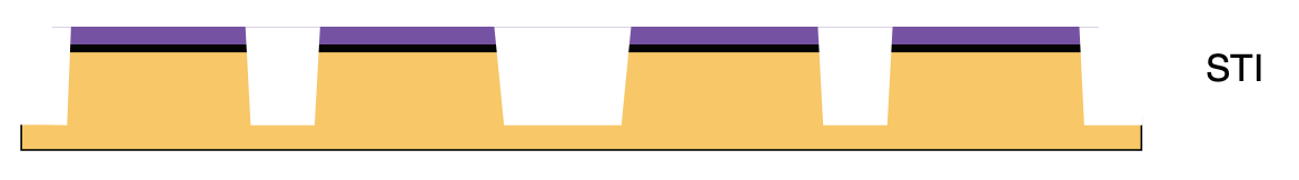
The purple is the SiN cap, the black is the oxide, and the yellow is the p-doped silicon. Those gaps are what we’ve just etched, the STI! Now, we will fill the trenches with oxide, a good dielectric (insulator), to isolate each future transistor. To do that, we deposit oxide via chemical vapor deposition (CVD). Deposition of material can happen a few different ways in chipmaking, and it’s good to know that CVD is one of them and is one of the “less precise” ways to deposit.
After the CVD of oxide, we will have “mountains” of oxide in our STI, as you can see below:
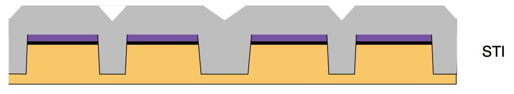
We don’t want mountains. We want relatively flat, uniform surfaces to work on so we can build on top of them. To flatten the oxide, we use chemical mechanical polishing (CMP). CMP polishes the surface using a slurry of chemicals and a polishing pad that spins over the wafer. After CMP, we can strip the SiN and oxide we originally formed, as they have served their purpose. Now, we’re left with a clearly defined AA!
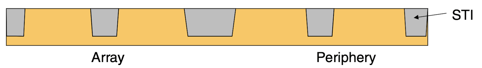
From a top-down perspective, the AA looks like below. Rectangles of AA separated from each other.
Form the Source and Drain (S/D) of Access Transistors
As you can see above, the AA is divided into two parts: the array and the periphery. The array is the section that accesses the capacitor, the device that stores memory. The periphery is the section that decides what capacitors need activating and amplifies their signals for readability. The two different functions means that the two sections have different design needs and components.
Now, we will start laying the groundwork for the access transistors in the array. These will become the switches that access the capacitors. By isolating the array sections with a mask, we blast the area with ions to make it more p-doped, forming a p-well. On top of that, we plant n-type dopants (opposite of p-type, so making the area negatively charged), to make the source and drain of the access transistors.
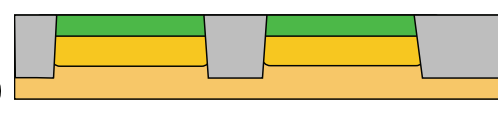
The green shows the n-type source and drain regions, with more bold yellow p-wells below it. The p-wells will prevent electrons from arbitrarily swimming to places we don’t want. After we finish the transistor, whenever we apply a voltage to the transistor’s gate, the well’s surface will flip charges, and electrons can swim from the source to the drain to turn the transistor “on.”
While we’re at it, we will perform a similar process on the periphery: here, we use masks to create a p-well and an n-well.
The reason the array has only p-wells while the periphery has both a p-well and an n-well goes back to their different functions. For an array, we need to maximize density. We want as many capacitors as possible to scale a DRAM chip, and the function of the array is relatively simple: store and fetch the data. Thus, in the array, we only build simpler nMOS transistors.
The periphery, on the other hand, conducts logic operations like deciding which capacitors need accessing. Thus, we will build more complicated CMOS transistors.
Make the Buried Wordline (BWL)
Next, we will make the wordline. The wordline is a device made of a conductive material like tungsten (W) that intersects with the array area. The wordline serves as the gate for the array transistors. If the DRAM chip were a spreadsheet, the wordline is the device that enables us to select a column. Later, we will make the bitline, which is how we select a row. If you have both, then you can select any cell, and grab its charge!
To make the wordline, we have to etch a place for it. Again, we form oxide and use masks to precisely etch the wordline into the array area. In this process, we are making a buried wordline (BWL); newer processes prefer this route of building the wordline directly into the silicon to reduce cell height, instead of making the wordline sit on top.
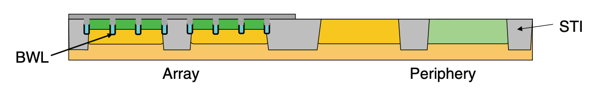
BWL etching is quite difficult, because we have to etch a very precise depth. We are also etching through AA (silicon) and non-AA (oxide like SiO2), and cutting through two different materials while controlling depth is doubly difficult. The etching leaves us with what is shown below, including the cross-sections of the AA and non-AA.
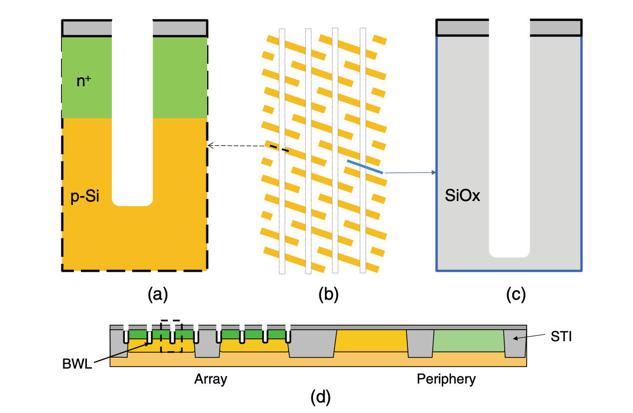
Note that two wordlines pass through the ends of each section of AA (the yellow rectangles in (b)). This is because we will form two cell transistors, and the middle will be a shared S/D for them. We will also later use the middle for bitline activities. You can see how economical we need to be with space for array transistors!
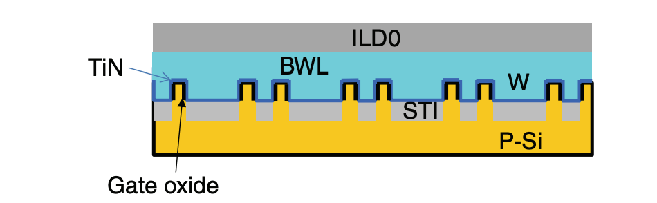
Next, we deposit the BWL material. In the holes formed, we deposit a thin layer of oxide, then titanium nitride (TiN), and then tungsten (W). The TiN is the gate electrode for the transistors, the switch that—when voltage is applied—permits electron flow from the source to the drain. The oxide is present to prevent the TiN from leaking into the silicon. The W is present for performance and conductivity purposes. The result is shown below.
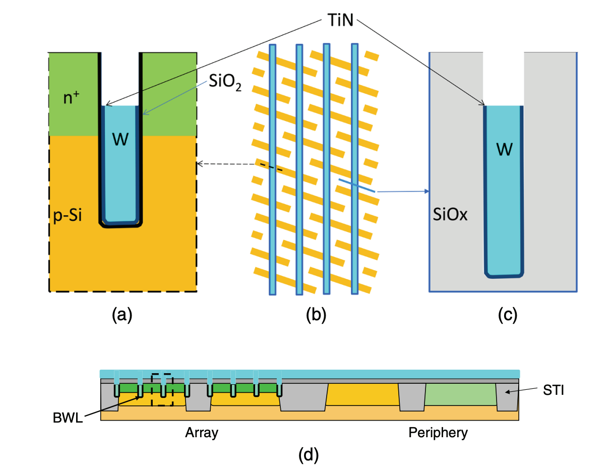
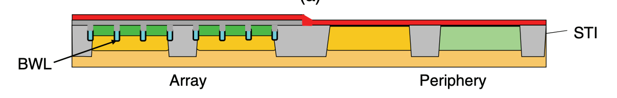
After making our BWL, we deposit a thick layer of oxide to seal it off from other devices. The oxide goes over the entire wafer; this is known as an interlayer dielectric (ILD), and we will be stacking multiple of them as we progress. Below is what we are left with after the deposition of the ILD (the gray). You can see the small blue portions representing the BWL.
Below is also a view of the cross-section along the BWL.
Deposit the Bitline Contact (BLC) and the Bitline (BL)
Next, we will make the bitline contact, the physical connection between the access transistor and the capacitor. This is one of the most difficult steps in the process, as we need very precise alignment of structures.
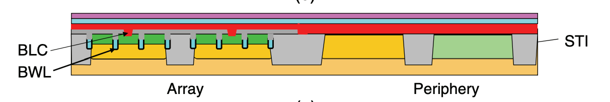
But first, you may have noticed that we have sealed off the periphery area with oxide before giving its transistors a S/D or gate. So first, we will use makes to partially etch the oxide, clearing to build on the periphery, as you can see below.
Then, we will deposit a gate oxide on top of the wells of the periphery transistors. Then, we will deposit an n-doped polysilicon over the entire AA, which will function as both the gate electrode for the periphery and the material for the bitline contact.
Because the polysilicon is n-doped, we can leave it alone over the p-well we formed in the periphery. However, we now have to use masks to conduct p-doping via ion implantation over the n-well portion. The region with an n-well and p-dope on top is known as the pMOS transistor, whereas the region with a p-well and n-dope on top is known as the nMOS (similar to the structure in the array) transistor. Together, they make a CMOS.
After the polysilicon deposition, we are left with what is below. The red is the polysilicon.
Now, we move onto the BLC. Because the polysilicon will form the BLC, we have to etch a path for it to connect with the array transistor. Thus, we will use masks to etch off the polysilicon over the array and etch the BLC through the ILD oxide. We have to carefully align the etching region with the array transistor’s S/D and not onto the BWL. After the etch, we redeposit the polysilicon; then, we also deposit a layer of W and TiN, which forms the bitline, and a SiN cap over that.
The teal is the bitline (BL), and the purple is the SiN. The bitline, composed of W and coated in TiN, is the carrier of charges from capacitors to the sense amplifiers in the periphery transistors that make the charge readable. The BL, as you can see, is also perpendicular to the WL. A top-down view of what we have is shown below.
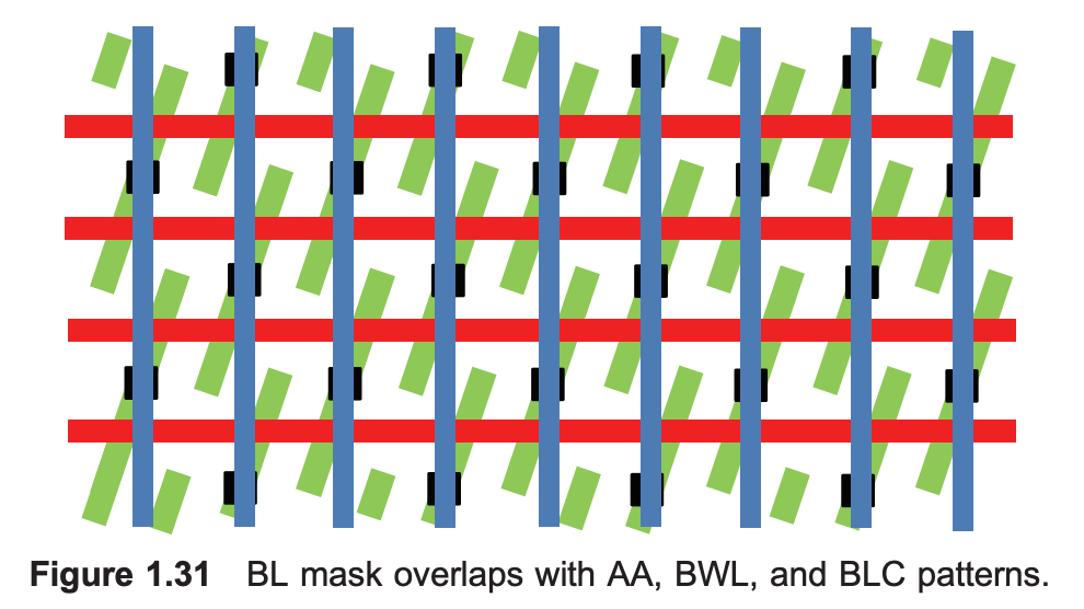
Here, the green area is the AA, the red lines are the BWL, the black box is the BLC, and the red lines are the BL.
Form the Sidewall Spacers for the Storage Node Contact (SNC)
After forming the BLC and the BL, we will form sidewall spacers for the storage node contact (SNC). Sidewall spacers are structures that will help prevent the future SNC from shorting to the BL. The SNC is the physical connection between the bitline and the storage node capacitor.
To make sidewall spacers, we will use a mask to expose the area in the array and etch back part of that polysilicon, bitline tungsten and titanium nitride, and silicon nitride we had just deposited. You will notice that a lot of chip-making is a lot of tortuous depositing just to etch and deposit again. Below is the section after that etching.

Then, we will deposit more SiN around the pillars of the spacers, which will form as a barrier for later etching. What’s left is below.

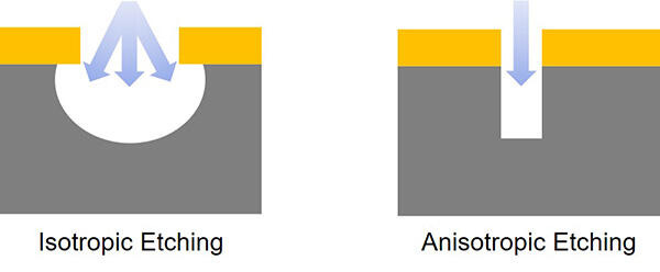
Then, we etch just enough SiN to leave gaps in between the pillars. This is known as anisotropic etch, and we have conducted it before when forming STI. Anisotropic etch deletes straight lines of materials, whereas isotropic etch cuts in every direction, forming more circular areas.
Below is the result of the anisotropic etch.

After the etch, we redeposit the ILD oxide and polish it via CMP. Then, we will etch the sidewall spacers by cutting through the oxide and creating little funnels from the gaps we created through the last anisotropic etch. This works because the chemical etch cuts through oxide very well but not well through SiN! The result is below.

Now, when it is time to make our SNC, it will be easy to align the deposition, as the sidewall spacers act as convenient, microscopic funnels! This is known as self-aligned contact (SAC).
Finish the Periphery Transistors
Before we can get to making the SNC, though, we first finish up the periphery transistors. To do that, we etch the ILD, polysilicon, BL, and SiN in the periphery except for what is over the gate oxide. Then, we use ion implantation to make the S/D in the nMOS and cMOS transistors (p-type in the n-well and n-type in the p-well). The result is below.
You don’t notice the sidewall spacers in the array in the diagram above because they are present behind the layered stack shown.
After the ion implantation, we deposit SiN and etch it back again to form sidewall spacers for the periphery. The sidewall spacers on the periphery will serve as funnels for a metal layer later on. The result is below.
Form the SNC
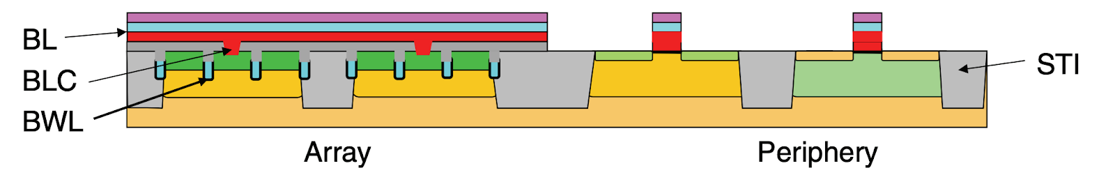
Now we are ready to form the SNC. First we deposit oxide over the entire AA and polish it. This layer of oxide is known as ILD1, and the layer we had before is referred to as ILD0. Then, we etch the holes for the SNC and for the M1. The M1, the first metal-interconnect layer, is deposited in the periphery area and acts as the electrical connection between the periphery transistors and other parts of the chip.
Then, we deposit TiN and W to fill those holes. After polishing it, the result is below. You can see that the SNC is behind the direct view and ranges from ILD0 to ILD1 while connecting at the access transistors’ S/D.
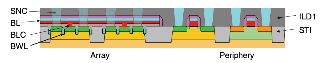
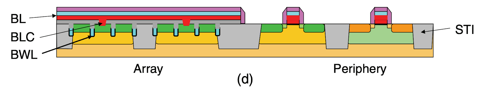
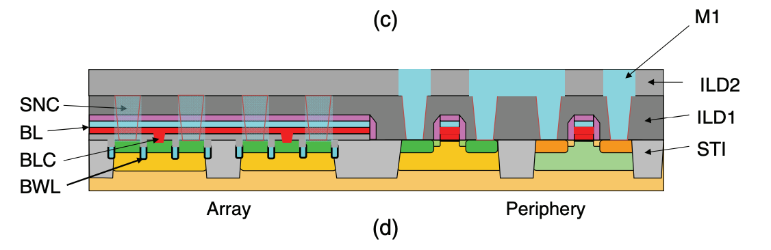
After this, we deposit another layer of oxide (ILD2), etch holes for M1, and deposit another more metal interconnect in the M1 hole. The result is below.
From the top-down, the DRAM chip looks like below:
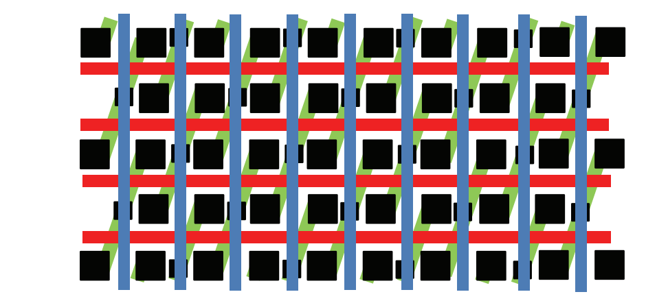
Our chip has now become very dense! You can see the intersecting BWL and BL, the BLC in the middle of the AAs, and the SNCs at the ends of the AAs.
Deposit the Storage Node (SN) Capacitor
Our last step in the front-end process for DRAM is forming the storage node (SN) capacitor. This is the device that actually holds the charge AKA bit AKA memory. Forming this is the hardest part of the DRAM making process.
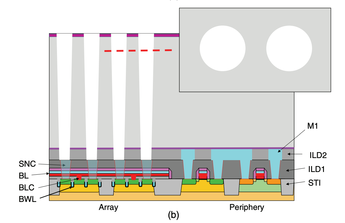
To make the SN capacitor, we first deposit SiN over the AA; this serves as an etch stop, which prevents us from etching too far when we make the capacitor holes. Then, you deposit a tall layer of ILD oxide, again capped with SiN. The result is below.
Using our SN capacitor mask, we will now etch the capacitor holes. This is the reason this step is the most difficult. The capacitor holes have very small critical dimensions, meaning their diameter is so narrow that there is little margin left for error. The pattern density is also high, as we are making and tightly packing many capacitor holes simultaneously. This creates more chance for error, as each hole may vary slightly, and some might be etched with unfixable defects. Lastly, the aspect ratio is very high, meaning the hole is very deep. Etching that deep can lead to a number of errors, as shown below.
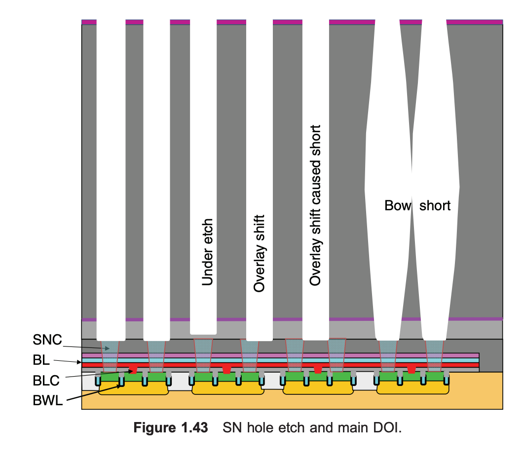
As shown, the ways to mess up SN capacitors are many and vary from misalignment to etch errors.
The result after successfully etching the capacitors is below.
After the etch, we deposit a thin layer of TiN, which will be the electrode of the SN capacitor that connects to the array transistor. Then, we apply photoresist all over the wafer. Photoresist is a liquid material that, when we later conduct destructive processes like etching or lithography, protects some areas of the wafer while leaving others exposed. We have been secretly applying and wiping off photoresist this entire time, but the application is particularly important in this instance. The structure after photoresist application is below.
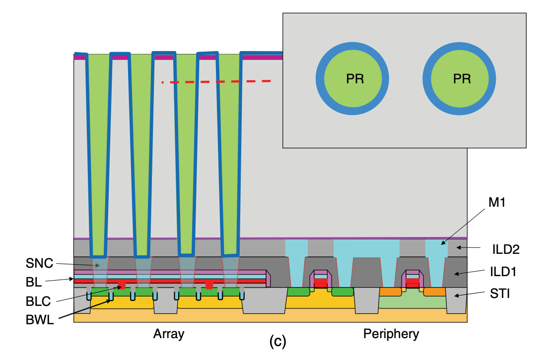
As you can see, the photoresist (PR) covers and protects the TiN inside the SN capacitor while exposing the TiN sitting on top of the SiN caps. Then, when we etch TiN, we can remove all TiN except for the TiN electrodes in the capacitors.
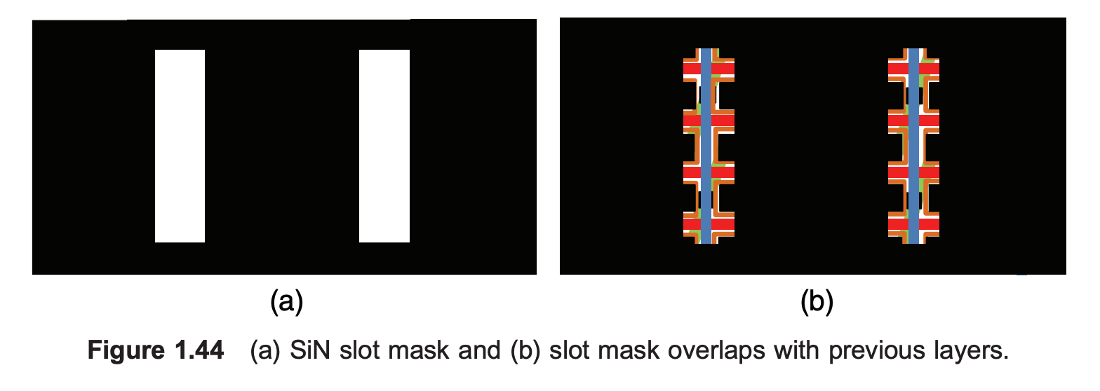
Then, we remove all SiN from the peripheral area and select portions of the array area using a slot mask. The slot mask is pictured below. We keep some of the SiN, as it serves as a prop to preserve the structural integrity of the capacitors. Without it, the capacitors would likely be too flimsy and collapse onto each other. The best metaphor I’ve seen is that the SiN caps act like the plastic rings on a six-pack of soda.
Then, we remove the oxide that was previously propping up the capacitors via an acid like hydrofluoric acid (HF). What’s left is below.
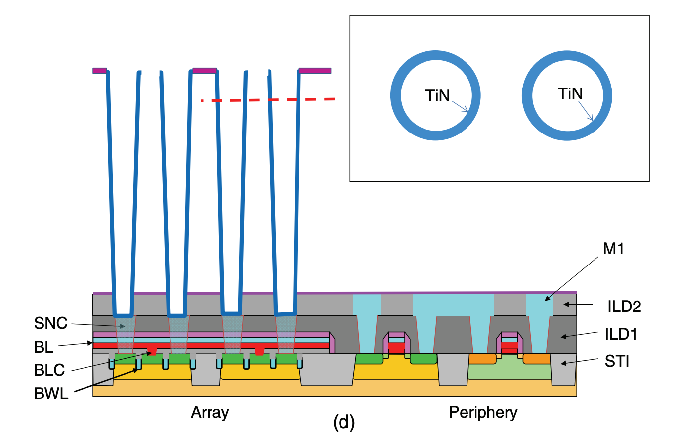
You can see the purple SiN propping up the bridge between capacitors, giving us maximal space everywhere else to work. Then, we deposit ZAZ dielectric film around our TiN in the capacitors. ZAZ is a sandwich of zirconium oxide and aluminum oxide that acts as a high-k dielectric for our capacitor. A high-k dielectric is an insulator with a high dielectric constant (so just a really good insulator).
The function of the ZAZ is integral to a capacitor. A simplified diagram of a capacitor is below. Ours are cylindrical, but the same principle applies for plates.
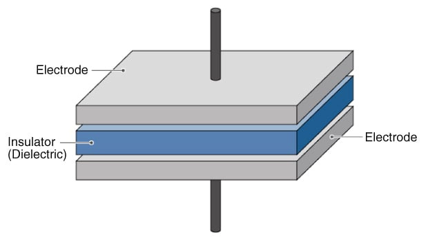
The dielectric between the electrodes, or conducting plates, on either side serves to enhance the capacitance—the ability to store charge—and prevents short circuits in a capacitor.
After dielectric ZAZ deposition, another thin layer of TiN is deposited to form the SN capacitor and serve as the electrode to ground, or plate electrode. The plate electrodes function as a “control” or baseline for when charge passes through the signal electrode. By comparing the voltage of the ground electrode versus the signal electrode, the signal electrode can be sensed.
Lastly, we deposit a filler conductor (usually SiGe) to fill any gaps to finish up the SN module! The finished DRAM layer is shown below.
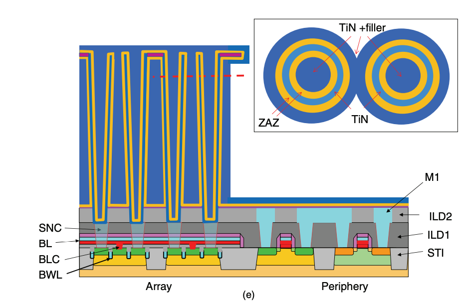
As you can see, the TiN with filler layer is the point that contacts with the SNC, which means that the TiN with filler is serving as the signal electrode for the capacitor.
The massive amount of conducting filler replacing where the oxide used to be is also a genius method for maximizing capacitance. Capacitance is equal to εAd, where ε is a constant, d is the distance between the electrodes (or basically thickness of the dielectric, or ZAZ), and A is the surface area of the electrodes. By maximizing the area of the filler, we increase the capacitance without having to trade off factors like height or depth!
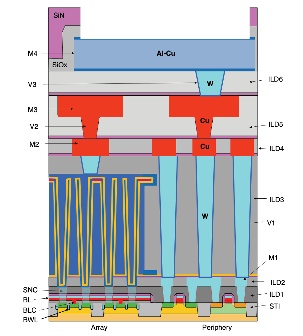
After all this is done, we have officially finished the front-end of the line process for DRAM. After this, more work is done on the back end to create metal interconnections in the periphery area so that everything works together. We won’t get into that, since we have covered the heart of DRAM making: the transistors and the capacitors.
For completeness and satisfaction, though, below is a complete diagram of the DRAM after the back-end processes.
Putting it All Together
We have walked through a lot of steps to get to this point, and the whole picture may have been easily lost throughout the process, so let’s review how each part works in tandem.
When the wordline (BWL) is turned on, the gates of the access transistors along that BWL all open. This connects the bitline (BL), accessed via the bitline contact (BLC), to the storage node contact (SNC), which in turn connects to the signal electrode inside the storage node (SN) capacitor. The charge in the capacitor is defined as the charge of the signal electrode relative to the baseline of the plate electrode—the outer TiN layer across the ZAZ dielectric. When connected, charge sharing occurs between the signal electrode and the BL: if the cell holds a “1,” the bitline voltage nudges up; if it holds a “0,” the bitline voltage dips slightly. This tiny change is detected and amplified by the sense amplifiers in the periphery transistors, restoring the cell and producing a full digital 0 or 1. Congratulations, you have read a singular bit in DRAM!
great article, and very nice illustrations.
When describing the wordline, you used a spreadsheet analogy, comparing the wordlines to selecting a column in a spreadsheet and the bitlines to selecting a row.
I know the spreadsheet row vs. column selection is arbitrary, but to make the analogy more accurate to how DRAM addressing works, I’d suggest to swap the row and column assignment. In real DRAM, when the customer inputs a Row address, that selects and activates a specific Wordline. Then when they Read or Write to a Column address, that selects a specific bitline (or more accurately a group of bitlines). Therefore, I would recommend to change the Wordline to be picking a “row” from the hypothetical spreadsheet, and the Bitline picking a “column”